TI��˾��DRV8305-Q1���������������õ�դ��������,�ṩ��������������,ÿ���������߱ߺ͵ͱ�N��MOSFET;��ɱ�������֧��100%ռ�ձ�.��������AEC-Q100��,4.4-V ��45-V������ѹ,դ����ֵ����1.25A��1A,�����¶ȨC40�浽150��,��Ҫ��������BLDC��PMSM����,�����ͱú�ˮ��,���Ⱥķ�綯��.���Ľ�����DRV8305-Q1��Ҫ����,���ܿ�ͼ,����Ӧ�õ�·ͼ�Լ�DRV8305-Q1EVM������������դ����������ģ����Ҫ����,��ͼ,��·ͼ�Ͳ����嵥.
The DRV8305-Q1 device is a gate driver IC for three-phase motor-drive applications. The device provides three high-accuracy half-bridge drivers, each capable of driving a high-side and low-side N-channel MOSFET. A charge pump driver supports 100% duty cycle and low-voltage operation for cold crank situations. The device can tolerate load dump voltages up to 45-V.
The DRV8305-Q1 device includes three bidirectional current-shunt amplifiers for accurate low-side current measurements that support variable gain settings and an adjustable offset reference.
The DRV8305-Q1 device has an integrated voltage regulator to support an MCU or other system power requirements. The voltage regulator can be interfaced directly with a LIN physical interface to allow low-system standby and sleep currents.
The gate driver uses automatic handshaking when switching to prevent current shoot through. The VDS of both the high-side and low-side MOSFETs is accurately sensed to protect the external MOSFETs from overcurrent conditions. The SPI provides detailed fault reporting, diagnostics, and device configurations such as gain options for the current shunt amplifier, individual MOSFET overcurrent detection, and gate-drive slew-rate control.
Device Options:
DRV8305NQ: Grade 1 with voltage reference
DRV83053Q: Grade 1 with 3.3-V, 50-mA LDO
DRV83055Q: Grade 1 with 5-V, 50-mA LDO
DRV8305NE: Grade 0 with voltage reference
DRV8305-Q1��Ҫ����:
AEC-Q100 Qualified for Automotive Applications
Ambient Operating Temperature Ranges:
Temperature Grade 0(E): �C40�� to 150��
Temperature Grade 1(Q): �C40�� to 125��
4.4-V to 45-V Operating Voltage
1.25-A and 1-A Peak Gate Drive Currents
Smart Gate Drive Architecture (IDRIVE & TDRIVE)
Programmable High- and Low-Side Slew-Rate Control
Charge-Pump Gate Driver for 100% Duty Cycle
Three Integrated Current-Shunt Amplifiers
Integrated 50-mA LDO (3.3-V and 5-V Option)
3-PWM or 6-PWM Input Control up to 200 kHz
Single PWM-Mode Commutation Capability
Serial Peripheral Interface (SPI) for Device Settings and Fault Reporting
Thermally-Enhanced 48-Pin HTQFP
Protection Features:
Fault Diagnostics and MCU Watchdog
Programmable Dead-Time Control
MOSFET Shoot-Through Prevention
MOSFET VDS Overcurrent Monitors
Gate-Driver Fault Detection
Reverse Battery-Protection Support
Limp Home-Mode Support
Overtemperature Warning and Shutdown
DRV8305-Q1Ӧ��:
Three-Phase BLDC and PMSM Motors
Automotive Fuel and Water Pumps
Automotive Fans and Blowers
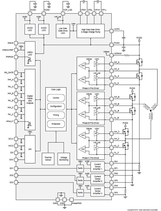
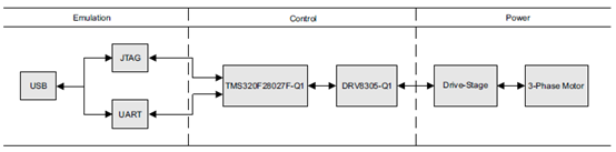
ͼ1.DRV8305-Q1���ܿ�ͼ
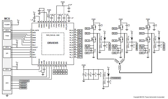
ͼ2.DRV8305-Q1����Ӧ�õ�·ͼ
DRV8305-Q1EVM������������դ����������ģ��
The DRV8305-Q1EVM evaluation module (EVM) is a 4.4 V to 45 V, 25 A, 3-phase motor drive and control system based on the DRV8305-Q1 automotive motor gate driver, TMS320F28027 motor control microcontroller, and CSD18540Q5B NexFET™ power MOSFET. The EVM allows for simple evaluation of the DRV8305-Q1 with a wide array of test points, interfaces, and configurability.
The EVM has onboard reverse battery protection, a regulated 3.3 V supply from the TPS7B6933-Q1 LDO, interface header for all control and feedback signals , and onboard XDS100v2 emulator. The EVM has individual DC bus and phase voltage sense as well as individual low-side current shunt sense for sensorless BLDC control algorithms. The drive stage is fully protected with short circuit, thermal, shoot-through, and undervoltage protection and is easily configurable via an SPI interface.
The EVM is ideal for evaluation and rapidly developing with the DRV8305-Q1, with primary software support through MotorWare using the InstaSPIN-FOC sensorless control solution.
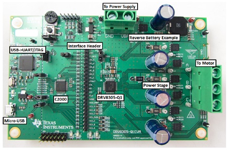
ͼ3.DRV8305-Q1EVM����ͼ
DRV8305-Q1EVM��Ҫ����:
4.4 V to 45 V Operating Supply Voltage Range
Supports up to 25 A Continuous Output Current
Provides Phase Voltage and Current Feedback ForSensorless BLDC Control Solutions
Complete Brushless DC Control and Drive Stage
Onboard XDS100v2 Emulator
What��s Included
DRV8305-Q1 Evaluation Board
Micro-USB Cable
ͼ4.DRV8305-Q1EVM��ͼ
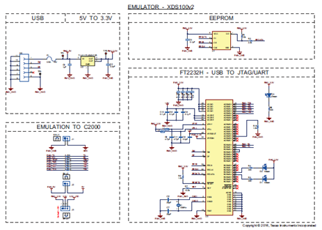
ͼ5.DRV8305-Q1EVM��·ͼ(1)
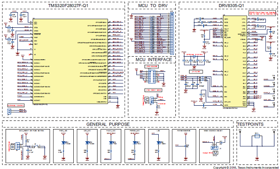
ͼ6.DRV8305-Q1EVM��·ͼ(2):MCU DRV
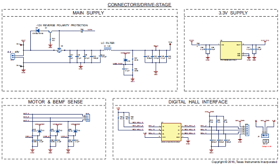
ͼ7.DRV8305-Q1EVM��·ͼ(3):��Դ
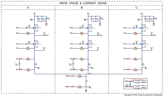
ͼ8.DRV8305-Q1EVM��·ͼ(4):��
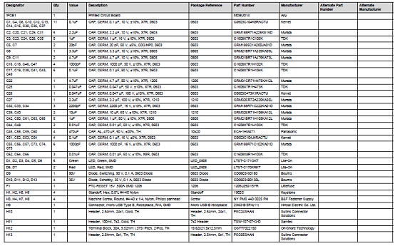
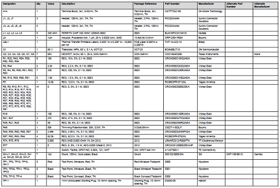
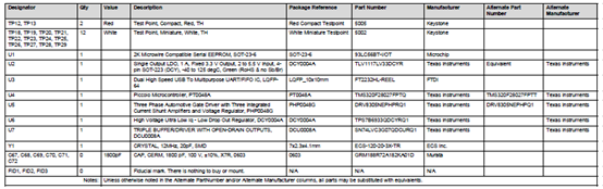
DRV8305-Q1EVM�����嵥:
|