| ��ǰλ�ã���ҳ->������� |
|
| L5963����LDO��HSD��˫·������ѹ��������� |
|
|
| ������Դ���������Ƽ� ����ʱ�䣺2018/1/22 11:50:00 |
������ѯ�� |
| |
ST��˾��L5963��˫·��Ƭ������ѹ��,������������ģʽͬ����ѹת����,������ѹ��Դ(LDO)�߱�������(HSD)�͵�ѹ�����.Ϊ�˱�֤³������,���е�������е������ȱ����͵�������.����AEC-Q100,�����ѹ��3.5V��26V,�����˸߱�/�ͱ�NDMOS,�������1V,���ص���3.0A,��Ҫ������������.���Ľ�����L5963��Ҫ����,���ܿ�ͼ��Ӧ�õ�·,�Լ�������EVAL-L5963��EVAL-L5963Q��Ҫ����,��·ͼ��PCB���ͼ.
The L5963 integrates two switching mode synchronous step down converters, a linearly regulated power supply, a protected high side driver and voltage detectors. To guarantee a robust operation, all the outputs have independent thermal protection and current limitation.
The two switching mode synchronous step-down converters employ voltage mode control and feed forward functions to provide good load regulation and line regulation. Each converter has its own enable. The users can adjust the output voltage of the two converters by an external resistor divider. If the converters need to work with a frequency different from the free running frequency, in order to consider EMC performance in system level, they can be synchronized to an external clock by applying it on the SYNCIN pin. The frequency should be higher than half of the free running frequency. If there are more than one L5963 in the system they can work in Master-Slave configuration, to make sure all L5963 have the same operating frequency of the Master device. This Master-Slave function is implemented by a dedicated pin SYNCOUT which always gives the operating frequency of DC/DC1.
A dedicated voltage detector is integrated in the first switching converter to monitor DC/DC1 output. When the output voltage of DC/DC1 goes above the threshold, SW1OK is released and goes back to high with configurable delay set by a capacitor on the SW1OKDLY pin.
The linear regulator can work as standby regulator with low Iqor as a non-standby regulator. Connecting its enable ENLDO to its supply VINLDO the regulator works as a standby regulator, while connecting ENLDO to a voltage lower than 5 V the regulator works as non-standby regulator, with higher load capability but also higher quiescent current.
In standby state, i.e. only the linear regulator is powered and works as a standby regulator, with a load below 100 ��A the device has a quiescent current of just 25 ��A.The small drop-out voltage of the linear regulator allows its use with low operating supply voltage.
In many cases, the linear regulator has to provide voltages to devices which need the reset function, like a MCU: this is provided by the LDOOK output, that is pulled low when VOUTLDO goes below a threshold. Once VOUTLDO returns above that threshold, with a specified hysteresis, LDOOK goes back to high with a configurable delay set by a capacitor on pin LDOOKDLY.
The high side driver is enabled by a dedicated pin and has a very low drop-out voltage. Protection circuits, like independent thermal protection, OCP, OVP and some special protections (loss of GND, SPU, short to supply and so on), are implemented to make it very robust.
L5963 also embeds a voltage monitor (VDOUT), adjustable by means of an external resistor divider, that can be used to sense the battery or other voltages in the system. Sensing voltage is fed to pin VDIN. For instance, VDOUT might be used to monitor the output of DC/DC2, realizing in this way the Power Good function for that block. VDOUT is pulled low when voltage on VDIN goes below the specified threshold. Once VDIN returns above that threshold, with a specified hysteresis, VDOUT goes back to high with a configurable delay set by a capacitor on pin LDOOKDLY
Two different packages are available. The PowerSSO-36 slug-down allows to dissipate the heat on the board and reduce the application size. The slug has to be connected to the ground plane. This is the package suggested for standard applications. When this is not enough, because the L5963 is used as pre-regulator for high consuming applications and both the 2 DC-DC are working at high currents, the PSSO36 slug-up allows the use of a heat-sink to make easier power dissipation.
L5963 is a dual step-down switching regulator with internal power switches, high side driver and a low drop-out linear regulator that can operate as standby regulator or normal LDO.
All the regulators can be connected directly to the vehicle battery. In addition to an adjustable voltage detector, voltage supervisors are available.
The two DC-DC converters can work in free-run condition or synchronize themselves to an external clock. DC/DCs��PWM outputs have a 180��phase shift.
The high operating frequency allowed by the synchronization input helps to reduce AM and FM interferences and grants the use of small and low cost inductors and capacitors.This IC finds application in the automotive segment, where load dump protection and wide input voltage range are mandatory.
A slug-up package option is available for applications which require heatsink use.In standby condition the device guarantees extremely low quiescent current (25 ��A typical @ -40��
L5963��Ҫ����:
AEC-Q100 qualified
Two step-down synchronous switching voltage regulators with internal power switches:
�C W ide input voltage range (from 3.5 V to 26 V)
�C Internal high-side/ low-side NDMOS
�C 1 V minimum output
�C 3.0 A load current
�C 250 kHz free-run frequency
�C 250 kHz < f < 2 MHz synchronization range
�C Integrated soft-start
�C Independent hardware enable pins
�C Independent power supply
�C 180�� PWM output phase shift
�C Programmable switching frequency divider by 1, 2, 4 or 8 between the two DC/DC regulators
�C Power good function
One standby / linear regulator
�C Output voltage programmable with external resistor divider
�C 250 mA maximum current capability
�C Backup function
�C Power good function
One high side driver
�C 0.5 V max drop @ 0.5 A
�C Protected against short to ground and battery, loss of ground and battery, unsupplied short to battery
Programmable under voltage battery detector
�C Under voltage threshold adjustable through dedicated pin (VDIN)
Load dump protection
Independent thermal protection on all regulators
Independent current limit on all regulators
Extremely low quiescent current in standby conditions
Power good / adjustable voltage detector outputs to realize customized power up/down sequences
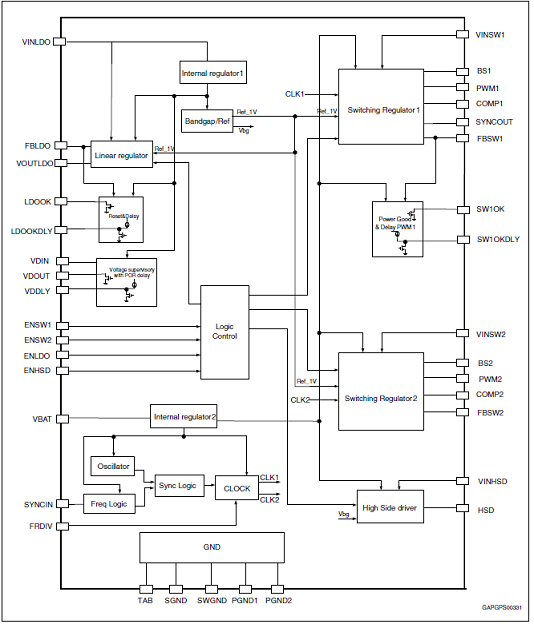
ͼ1.L5963���ܿ�ͼ

ͼ2.L5963����Ӧ�õ�·ͼ
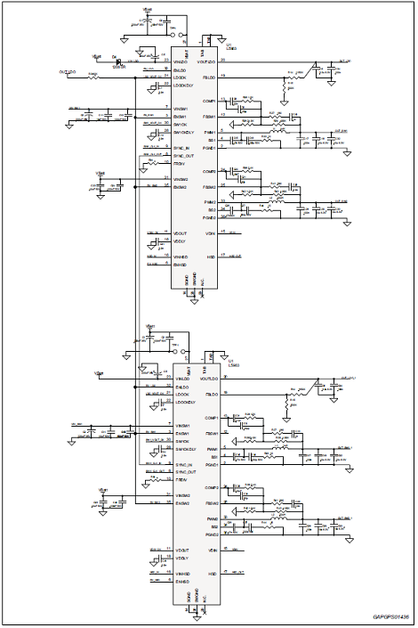
ͼ3.����L5963Ӧ�õ�·ͼ
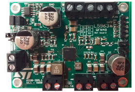
������EVAL-L5963��EVAL-L5963Q
EVAL-L5963 and EVAL-L5963Q are two evaluation boards supporting the multichannel voltage regulator L5963 in PowerSSO-36 slug down and VQFPN-48 packages respectively. The boards offer the flexibility to independently supply the various regulators and to work at a frequency up to 2 MHz.
������EVAL-L5963��EVAL-L5963Q��Ҫ����:
DC-DC1 working at 1.2 V, 2 MHz
DC-DC2 working at 5 V, 250 kHz
Input connector to sync a different working frequency up to 2MHz
Oscillator on board to change working frequency up to 2MHz
DC-DC1 and DC-DC2 working up to 3A
LDO working at 3.3 V, 250 mA
Possibility to change output voltages
Jumpers to enable or disable DC-DC
Jumpers to enable or disable LDO
Pins to independently supply DC-DC1 and DC-DC2 together with LDO
Output connectors to check output voltages
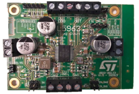
ͼ4.������EVAL-L5963����ͼ
ͼ5.������EVAL-L5963Q����ͼ
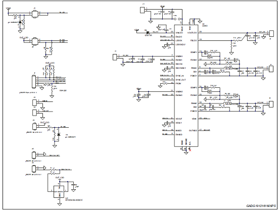
ͼ6.������EVAL-L5963(PowerSSO-36��װ)��·ͼ
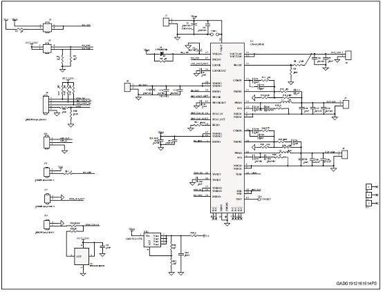
ͼ7.������EVAL-L5963Q(VQFPN-48��װ)��·ͼ
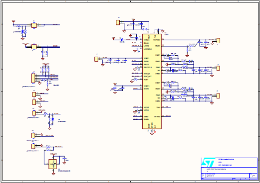
ͼ8.������EVAL-L5963��·ͼ
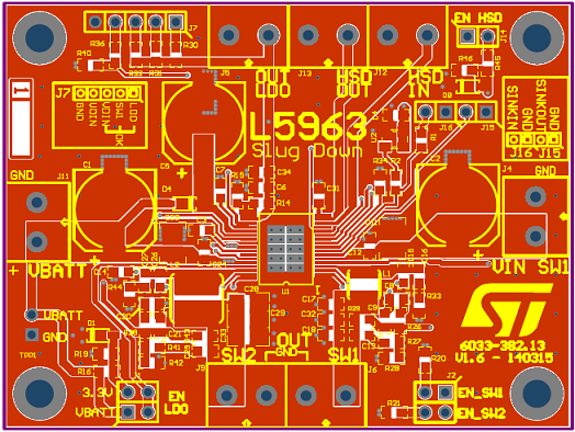
ͼ9.������EVAL-L5963 PCB���ͼ |
| |
|
|
|
|
|
| |
| |
| |
 |
�����ܶ����²�Ʒ����Ȥ |
 |
|
 |
| ��Ʒ�ͺ� |
���ܽ��� |
�����ͺ� |
��װ��ʽ |
������ѹ |
��ע |
| HT7178 |
�����ѹ��Χ��2.7V -14 V;�����ѹ��Χ��4.5V-20V
;�ɱ�̷�ֵ������ 14A
|
TPS61088/HT7167 |
DFN-20 |
2.7V-14V |
20V 14A������ضϵ�ȫ����ͬ����ѹIC |
| HT317 |
2X42W/18V/4����75W/24V/4�� |
|
TSSOP-28 |
5V-26V |
42W������/75W������D���IC,��������ѹ5-26V��������ѹ32V�� |
| CS5080 |
CS5080E��һ��5V����,֧��˫��﮵�ش���Ӧ��,����ӵ�ص���ѹ������IC.CS5080E���ɹ���MOS�������첽���ؼܹ���ʹ����Ӧ��ʱ���輫�ٵ���Χ����������Ч�������巽���ߴ磬����BOM�ɱ���CS5080E����ѹ���س��ת�����Ĺ���Ƶ��Ϊ600KHz���2A�����磬ת��Ч��Ϊ90%�� |
|
ESOP-8 |
3.44V-7.0V |
5V USB���롢˫��﮵�ش���Ӧ�á���ѹ������IC |
|
| |
|
| |
|
|