TI��˾��TPS61094�Ǵ���·���ص�ͬ��˫��ѹ/��ѹת����,���п������ѹ��Χ�������ѹ,�ߴ�5.5V.��TPS61094�����ڽ�ѹģʽ���������ݳ��,���������յ��ѹ����������ӵ���ɱ��, ��TPS61094��������ѹģʽ,�����ѹ�������һ��������.���Զ���ѹ����ѹģʽ(EN = 1, MODE = 1),�������Դ�ӵ�ʱ,������·�����ѹ�����,ͬʱ�ܶԱ��ݳ������ݽ��г��.�������Դδ���ӻ�������Ŀ���ѹ, TPS61094������ѹģʽ,�ӱ��ݳ������ݵ��������ѹ.������ģʽ, TPS61094����60nA��̬����.����֧����ض�ģʽ(EN= 0, MODE = 1)��ǿ����ͨģʽ(EN = 0, MODE = 0).����ض�ģʽ, TPS61094��ȫ�����Ӹ��غ������Դ.��֧��ǿ����ͨģʽ,����ֱ��ͨ����·�������Ӹ��ص������ѹ,����������4nA����,�Ի�ó��������.��������·���ص���Ϊ 100-m��,����Ƶ��Ϊ1MHz.�������������·�������ȹضϱ���.����2mmx3mm 12����WSON��װ.��Ҫ����������ˮ��,�ֳ�ҽ���豸�������ջ�.���Ľ�����TPS61094��Ҫ����, ���ܿ�ͼ,���ֵ���Ӧ�õ�·, ����ģ��TPS61094EVM-066��Ҫ����,��·ͼ,�����嵥��PCB���ͼ.
The TPS61094 is a synchronous bi-directional buck/boost converter with bypass switch. The device provides a power supply solution for smart meter and super capacitor backup power applications.
The TPS61094 has a wide input voltage range and output voltage up to 5.5 V. When the TPS61094 works in Buck mode and charges the supercap, the charging current and the termination voltage are programmable with two external resistors. When the TPS61094 works in Boost mode, the output voltage is programmable with an external resistor.
During automatic Buck or Boost mode (EN = 1, MODE = 1), when the input power supply is applied, the device bypasses the input voltage to the output while it is capable of charging a backup supercap.
When the input power supply is disconnected or lower than the output target voltage, the TPS61094 enters Boost mode and regulates output voltage from a backup supercap. The TPS61094 consumes 60-nA quiescent current in this mode.
The TPS61094 supports True shutdown mode (EN= 0, MODE = 1) and the Forced bypass mode (EN = 0, MODE = 0). In True shutdown mode, the TPS61094 completely disconnects the load from the input supply. When supporting Forced bypass mode, the TPS61094 connects the load to the input voltage directly through a bypass switch and only consumes 4-nA current to achieve long battery life.
TPS61094��Ҫ����:
• Wide voltage range and current range
�C 0.7-V to 5.5-V input voltage range
�C 1.8-V minimum input voltage for start-up
�C Programmable boost output voltages, 2.7-V to 5.4-V setting range
�C Programmable buck charging termination voltages, 1.7-V to 5.4-V setting range
�C Programmable buck charging output currents, 2.5-mA to 600-mA setting range
• Ultra-low quiescent current
�C 60 nA in boost mode or buck charging mode
�C 4 nA in forced bypass mode
• High efficiency and power capability
�C Minimum 1.4-A inductor valley current limit
�C Two 60-m�� (LS) / 140-m�� (HS) MOSFETs
�C 100-m�� bypass switch resistance
�C 1-MHz switching frequency
�C Auto snooze mode operation at light load
�C Up to 92.3% efficiency at VIN = 3 V, VOUT = 3.6 V, and IOUT = 10 ��A
�C Up to 96.3% efficiency at VIN = 3 V, VOUT = 3.6 V, and IOUT = 100 mA
• Four operation modes controlled by the MODE and EN pins
• Rich protection
�C Output short-circuit protection
�C Thermal shutdown protection
• 2-mm �� 3-mm 12-pin WSON package
TPS61094Ӧ��:
• Gas meter, water meter
• Portable medical equipment
• Energy harvest
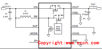
ͼ1. TPS61094����Ӧ�õ�·(1)
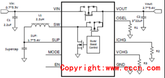
ͼ2. TPS61094����Ӧ�õ�·(2)
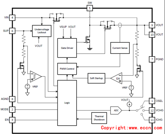
ͼ3. TPS61094���ܿ�ͼ
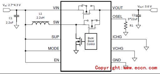
ͼ4. TPS61094﮵��3.6V����·��ѹת����Ӧ�õ�·(1)
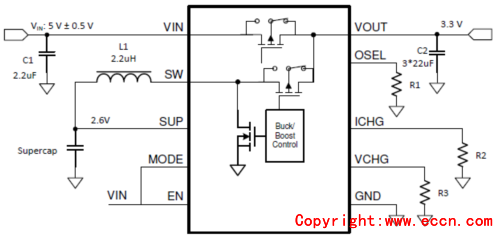
ͼ5. TPS61094 5V����3.3V��ѹת�������Զ���ѹ����ѹ����(2)
����ģ��TPS61094EVM-066
This users guide describes the schematic, layout, bill of materials (BOM), and setup of the evaluation module (EVM) for the TPS61094EVM-066. It can supply the Vout to programed target from 2.7 V~5.4 V with Vin low to 1.8 V. The TPS61094EVM-066 supports four operating modes with different jumpers configuration, including force bypass, true shotdown, force buck, and auto buck or Boost.
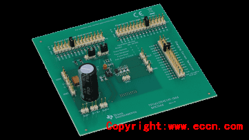
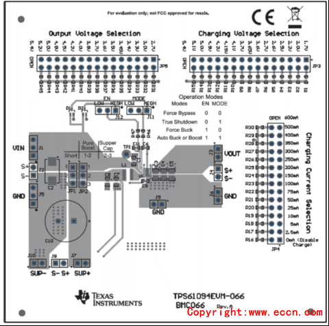
ͼ6. ����ģ��TPS61094EVM-066����ͼ
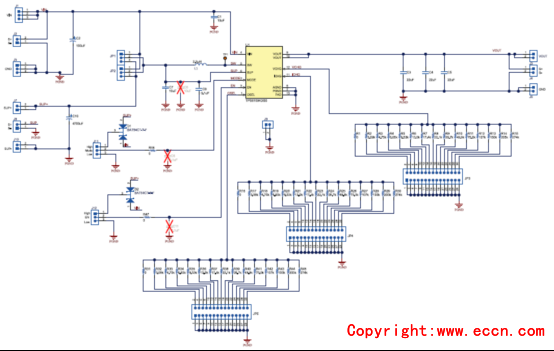
ͼ7. ����ģ��TPS61094EVM-066��·ͼ
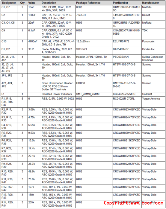
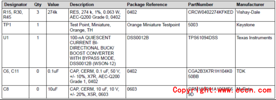
����ģ��TPS61094EVM-066�����嵥:
ͼ8. ����ģ��TPS61094EVM-066 PCB���ͼ:���㲼��
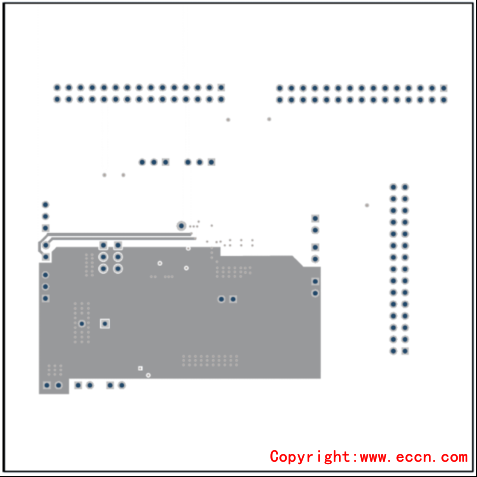
ͼ9. ����ģ��TPS61094EVM-066 PCB���ͼ:�ڲ�1����
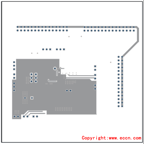
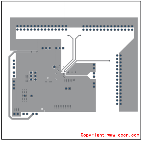
ͼ10. ����ģ��TPS61094EVM-066 PCB���ͼ:�ڲ�2����
ͼ11. ����ģ��TPS61094EVM-066 PCB���ͼ:�ײ㲼�� |